In modern electronics manufacturing, soldering rework remains one of the most persistent and preventable inefficiencies affecting productivity, reliability, and cost control. As printed circuit boards become increasingly compact, multilayered, and component‑dense, even minor design miscalculations can lead to solder bridging, tombstoning, insufficient wetting, or thermal stress fractures during assembly. Advanced Rework Technology addresses these challenges by providing the training and methods needed to reduce errors and improve overall manufacturing outcomes.
These defects are rarely isolated to workmanship alone; they are frequently embedded within the initial layout decisions of the board itself. Structured electronics training courses in the UK, therefore, play a decisive role in equipping engineers, PCB designers and soldering professionals with the technical competence required to integrate design for manufacturability principles at the earliest stages of development.
By strengthening foundational knowledge in PCB design courses and soldering technology, organisations can systematically reduce rework cycles, preserve solder joint integrity and enhance overall assembly yield.
The True Cost of Soldering Rework in Electronics Manufacturing
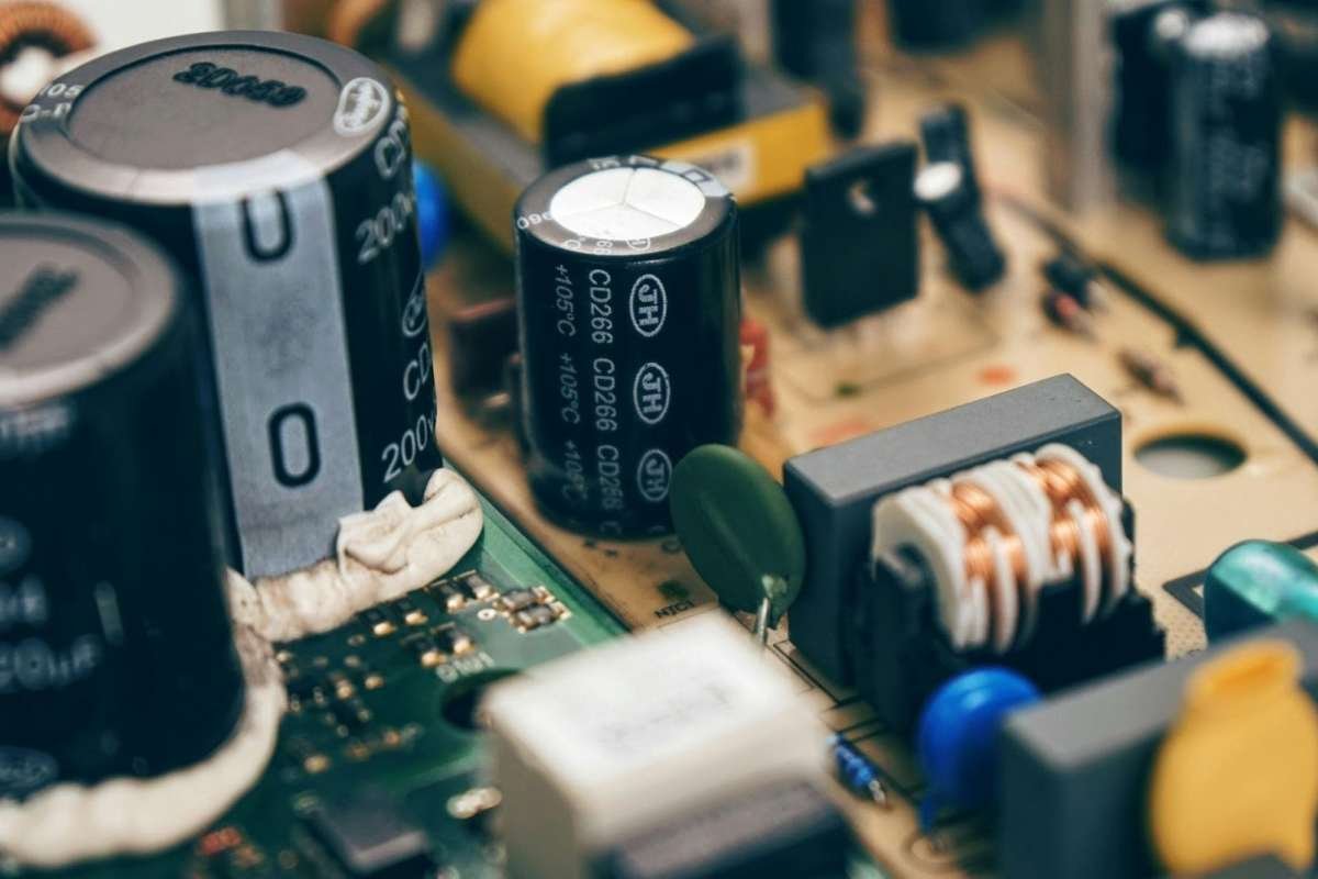
Soldering rework represents a substantial yet often underestimated burden within electronics manufacturing environments. While the visible impact is typically measured in additional labor hours and production delays, the deeper technical implications extend to material degradation, thermal fatigue, and cumulative handling stress on sensitive components. Advanced Rework Technology provides the training and solutions needed to address these issues, helping manufacturers reduce inefficiencies and protect component reliability.
Each rework intervention subjects the PCB to additional thermal cycling, which can compromise laminate integrity, weaken plated through-holes and accelerate intermetallic compound growth within solder joints. In high-density assemblies incorporating fine-pitch components, BGAs or QFNs, repeated thermal exposure increases the risk of pad lifting, delamination and micro-cracking, ultimately reducing long-term reliability.
For this reason, adherence to recognised PCB design guidelines is critical in preventing design-stage oversights that later manifest as soldering defects.
From an operational perspective, rework disrupts process stability and undermines first-pass yield performance. Instead of flowing seamlessly through solder paste printing, placement and reflow stages, assemblies requiring correction re-enter the production cycle, consuming additional machine capacity and skilled technician time.
This interruption reduces throughput efficiency and inflates overall manufacturing cost per unit. Within the soldering sector, it is widely recognised that many of these defects originate not from the soldering process itself but from preventable PCB layout oversights, reinforcing the strategic importance of advanced PCB design courses in reducing avoidable rework and preserving production consistency.
How PCB Design Directly Influences Solder Joint Integrity?
The integrity of a solder joint is fundamentally determined long before molten alloy ever contacts a component lead. PCB design parameters such as land pattern geometry, annular ring dimensions, solder mask clearance, and copper distribution directly influence wetting behavior, heat transfer efficiency, and surface tension balance during reflow or wave soldering. Advanced Rework Technology emphasizes these design fundamentals, ensuring that training and process improvements reduce defects before they occur.
Inadequate pad sizing can result in insufficient solder volume, while excessive copper planes without appropriate thermal relief may create uneven heating profiles that compromise metallurgical bonding. In fine-pitch assemblies, even marginal deviations in spacing tolerances can promote solder bridging or incomplete fillet formation, particularly where stencil aperture design has not been harmonised with the underlying layout.
Component placement strategy also exerts a measurable influence over solder reliability. As board complexity increases, designers must account for thermal mass variation across multilayer substrates, ensuring that temperature gradients do not induce differential expansion or warpage during the soldering cycle.
Poorly distributed high‑mass components may shadow adjacent devices, altering reflow dynamics and increasing the probability of cold joints or voiding beneath area‑array packages. Comprehensive PCB design courses emphasize these interactions between layout architecture and soldering technology, embedding design‑for‑manufacturability principles that minimize defect propagation and enhance long‑term assembly robustness. Advanced Rework Technology builds on these principles, offering training and solutions that help manufacturers anticipate layout challenges and reduce rework before defects occur.
IPC Standards and Professional PCB Design Courses
Within the soldering sector, IPC standards provide the technical framework that governs workmanship, acceptability criteria and repair methodology across the electronics manufacturing lifecycle. Standards such as IPC-A-610 define the visual and dimensional requirements for solder joint acceptability, while IPC-2221 establishes foundational principles for PCB design, including conductor spacing, creepage distances and land pattern configuration.
IPC-7711/7721 further formalises rework and repair procedures, outlining controlled techniques intended to preserve board integrity during corrective intervention. However, adherence to these standards requires more than procedural familiarity; it demands a comprehensive understanding of how design decisions interact with soldering technology and assembly constraints.
Professional PCB design courses translate these formal requirements into applied engineering competence. By integrating standards-based instruction with practical layout analysis, thermal management considerations and defect prevention strategies, structured training enables designers and technicians to anticipate soldering challenges before they manifest on the production line.
For organizations operating in safety‑critical sectors, where compliance and traceability are paramount, embedding IPC‑aligned expertise within the workforce strengthens quality assurance frameworks and reduces dependency on reactive rework processes. In this context, PCB training becomes not merely educational enrichment but a mechanism for safeguarding reliability, regulatory conformity, and manufacturing precision. Advanced Rework Technology supports these goals by equipping teams with the skills and processes needed to minimize defects and maintain the highest standards of production integrity.
Advanced PCB Training as a Strategic Manufacturing Investment
In contemporary electronics manufacturing, investment in advanced PCB design courses should be regarded as a deliberate strategy for operational optimization rather than an ancillary training expense. Soldering rework is inherently symptomatic of upstream design inefficiencies, and when organizations prioritize technical education in PCB layout principles, they effectively intervene at the root cause of recurring defects. Advanced Rework Technology reinforces this approach by equipping engineers with the skills and processes needed to minimize rework and strengthen long‑term manufacturing performance.
By embedding knowledge of pad stack configuration, impedance control, thermal balancing and component orientation within the design function, manufacturers can significantly enhance first-pass yield and stabilise process capability. This proactive alignment between design engineering and soldering technology reduces reliance on corrective intervention and preserves the structural integrity of the board throughout its lifecycle.
Furthermore, advanced PCB training cultivates a culture of technical accountability across multidisciplinary teams. When designers possess a sophisticated understanding of assembly tolerances, stencil design interaction and reflow dynamics, communication between design, production and inspection departments becomes materially more precise.
This cohesion supports lean manufacturing objectives by eliminating avoidable waste, shortening iteration cycles and improving product consistency across batches. In highly competitive markets where reliability and performance differentiation are decisive, organisations that embed rigorous PCB design education within their engineering infrastructure position themselves to achieve sustained reductions in soldering rework while reinforcing long-term manufacturing resilience.
Conclusion
Reducing soldering rework with PCB training represents a decisive shift from reactive correction to engineered precision within the electronics manufacturing sector. By integrating advanced PCB design courses into organizational development strategies, manufacturers equip designers and soldering professionals with the technical insight required to embed design‑for‑manufacturability principles at source. Advanced Rework Technology reinforces this approach, ensuring that training translates into fewer defects, stronger reliability, and long‑term operational efficiency.
This alignment between PCB layout architecture, IPC standards compliance and practical soldering technology strengthens first-pass yield, protects solder joint integrity and reduces unnecessary thermal stress on assemblies. In a landscape defined by miniaturisation, regulatory scrutiny and uncompromising reliability demands, structured PCB education serves as a foundational mechanism for eliminating avoidable defects and sustaining long-term production excellence.
Read Next: The Role of Leadership in Employee Training Programs